KiCad template review
Status: template ready to use, 2026-10-16. Project note: project-template. Procedure: ../sops/docs/SOP-021-new-pcb-design.
The EmbeddedEra KiCad 10 project template (template/EmbeddedEra_Project in the KiCad library) was checked and fixed on 2026-10-15 and 2026-10-16. Every change was proven with KiCad's own tools before it was pushed. The netlist has the same 47 nets with the same pins. ERC and DRC are clean apart from the expected warnings on an unfinished reference circuit. kicad-tidy-check reports 0 overlaps on every sheet, and the library's kicad-check gate ran on each push.
To start a board
- Pull the KiCad library.
- Copy
template/EmbeddedEra_Projecttohardware/<board>/. Rename theEmbeddedEra_Project.*files to the board name, includingEmbeddedEra_Project.kicad_dru. KiCad only loads the rule file that matches the project name. A rule file left with the old name drops every house rule without a warning. - Set the text variables: Project_Name, Customer, Part_Number (the board's EE-P number) and Revision (starts at A).
- The sheet files
Power,MCUandControlskeep their names. Add sheets as the board grows.
Before: one flat sheet
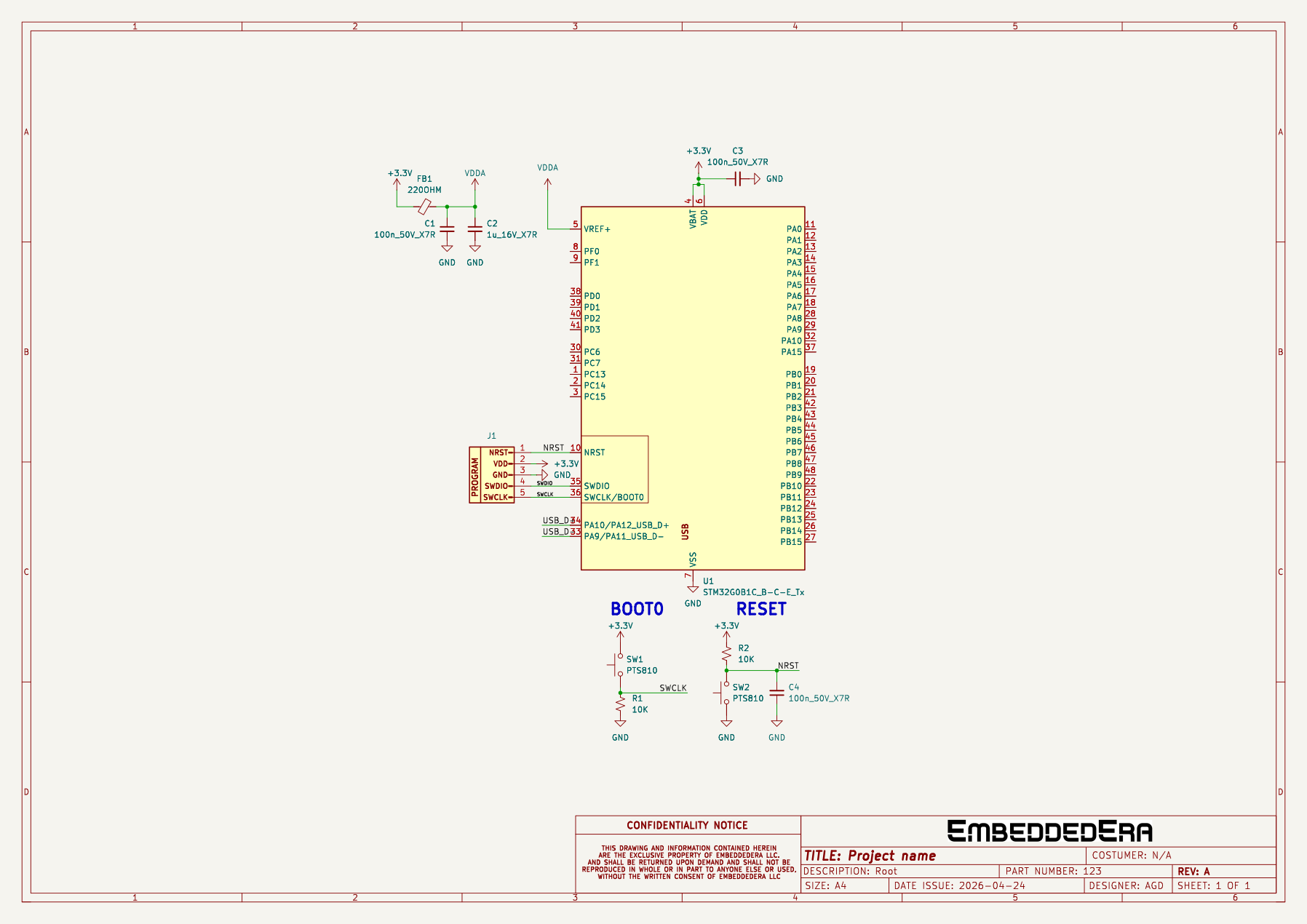
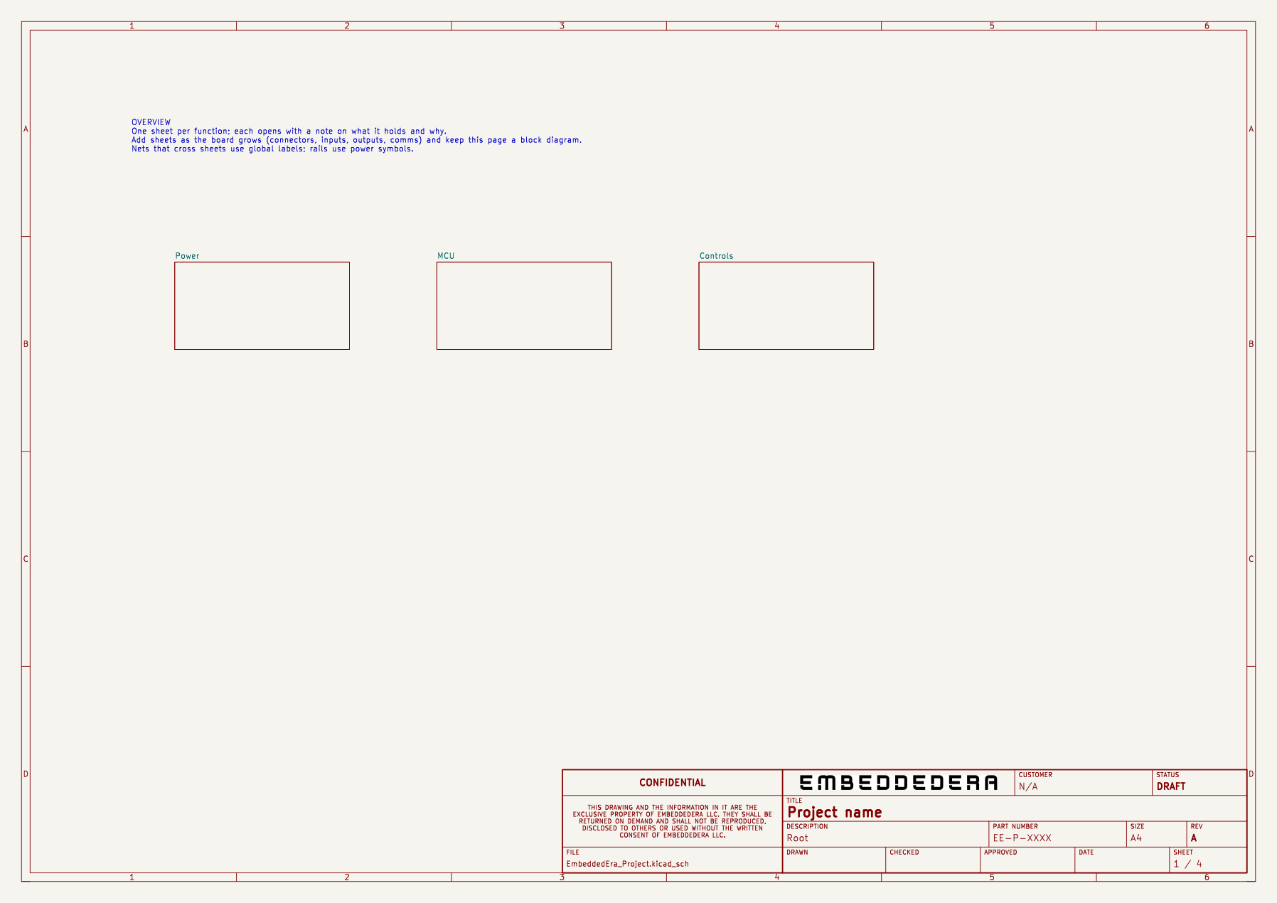
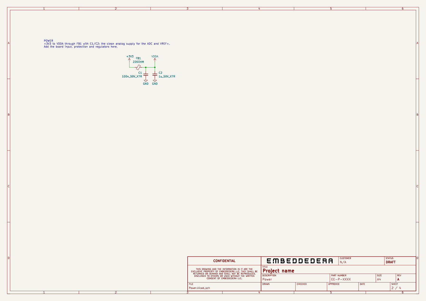
After: split by function
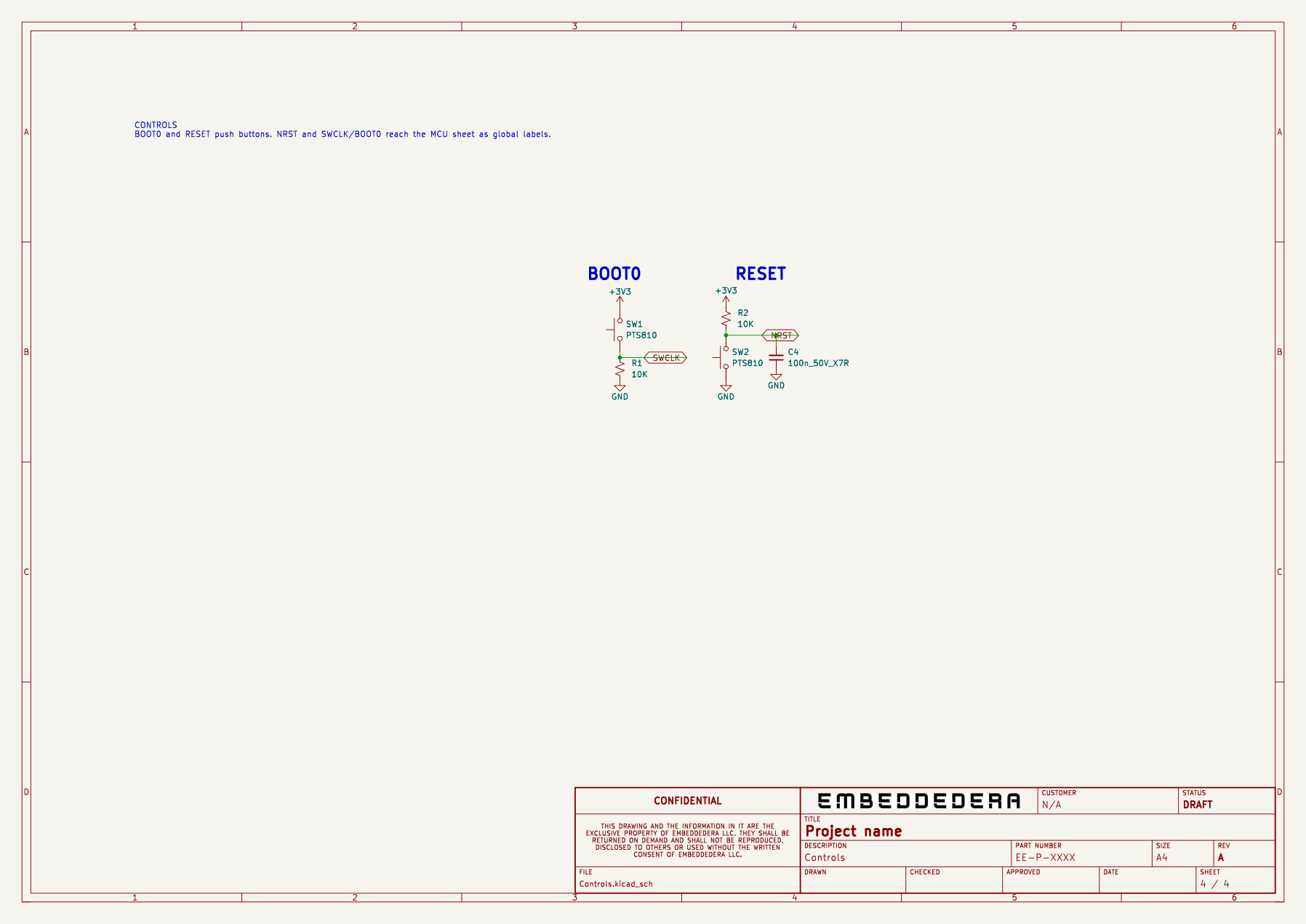
The root page is the overview. Each sheet opens with a note on what it holds. Nets that cross sheets are global labels (NRST, SWCLK, SWDIO, USB_D+, USB_D-), so they keep plain names and the USB2 net class still finds the USB pair.
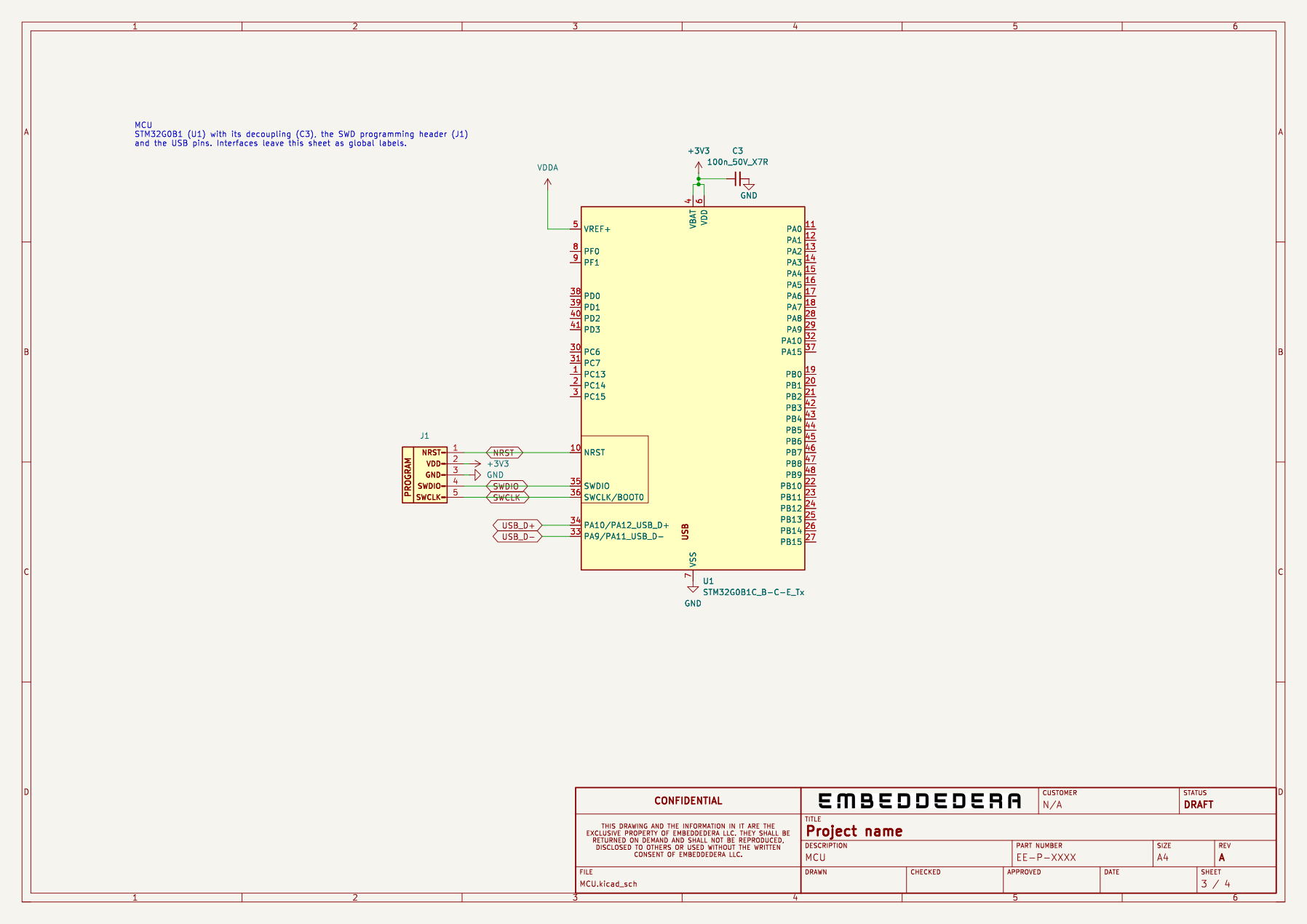
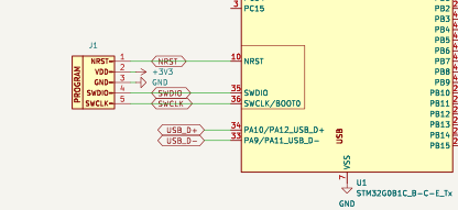
The programming header was moved left so its labels stop crowding the MCU pin numbers:
Title block (worksheet 005)
Rebuilt on one grid, with a small caption over each value, against the title-block contract in the 2026-09-16 engineering audit (fields after ISO 7200). New fields: CHECKED, APPROVED, STATUS and a release DATE shared by every sheet and the PCB, plus the FILE name. Designer no longer defaults to AGD. Status reads DRAFT, and Checker, Approver and Date stay empty until review (SOP-021 steps 2 and 12). The notice keeps its meaning with the grammar fixed. The logo is the v2 hex mark beside the wordmark, on a transparent background so it sits on the sheet colour instead of a white box.
Before:

After (template placeholders):

Logo on the board
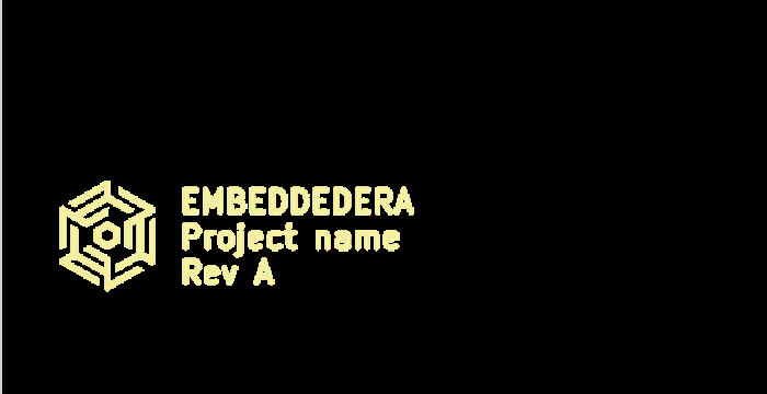
The front silkscreen carries the EmbeddedEra hex mark beside the board name and revision. Four footprints are in EmbeddedEra_Library: EmbeddedEra_Logo_Mark_5mm and _8mm, EmbeddedEra_Logo_Lockup_15mm and _25mm. They are board-only and stay out of the BOM and the placement file.
What changed
| Change | Proof | Commit |
|---|---|---|
| USB_D+ and USB_D- get the USB2 net class automatically | KiCad's own net-class lookup | 2e1fb4a |
| Revision starts at A; the README lists all 9 net classes and the rule-file rename | — | 2e1fb4a |
| Logo footprints; the template board carries the mark | DRC 0, silkscreen width measured | 0275789 |
| Stale symbols refreshed from the library (pins checked identical first) | netlist identical | 9692994 |
| Part numbers from the ERP on every part: U1 EE-C-0196, R1/R2 EE-C-0166, C1/C3/C4 EE-C-0012, C2 EE-C-0195, SW1/SW2 EE-C-0179, FB1 EE-C-0174, J1 EE-C-0065 | netlist fields | 9692994 |
| C2 is now 1u 50V X7R (the ERP has no 1u 16V part) | — | 9692994 |
Rail renamed +3.3V → +3V3 (house naming) |
the only net-name change | 9692994 |
| BOOT0 heading moved off U1's GND label | overlap check 1 → 0 | 9692994 |
| Title block worksheet 004 reads CUSTOMER (003 kept for older boards); PCB title shows the project name | — | 9692994 |
| Schematic split into Overview, Power, MCU, Controls | netlist identical, tidy-check 0 overlaps | a9a6012 |
| Logo v2: title-block wordmark and silkscreen footprints | DRC 0, silkscreen width measured | 76a9375 |
| Title block 005: one grid, review fields, shared release date, notice grammar | rendered on schematic and PCB | b2164fa |
| Title-block logo: hex mark + wordmark, transparent (was a white box) | rendered on the sheet colour | 5aedc4e |
Still open
Nothing. The J1 ERP status and the passive-library part numbers were set aside by the owner on 2026-10-16.